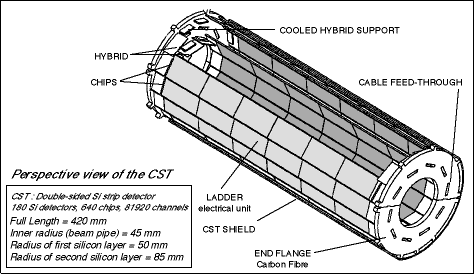
Figure 2a: H1 Central Silicon Tracker
2.1.1 Central Silicon Tracker
The CST consists of two layers of double sided silicon strip detectors. The inner layer (radius 50 mm) is a regular prism with 10 faces; the outer layer (radius 85 mm) is similar with 16 faces. Each face consists of six silicon detectors, of total length 360 mm, with readout at both ends. The strip pitch in phi is 25 um and in z is 90 um.
The resolution is 70 um for the impact parameter at 1 GeV/c and 80 um in z at 1 GeV/c.
Figure 2a: H1 Central Silicon Tracker
2.1.2 Backward Silicon Tracker
The BST consists of 8 discs (four in phase 1) mounted perpendicular to the beam line at distances between 280 mm and 860 mm from the nominal interaction point in the electron direction. The discs have an inner hole of 55 mm radius and are segmented into 16 azimuthal sectors with an outer radius of 125 mm.
In the final phase each disc is built as a composite of three different silicon layers. One has a pad segmentation for triggering. The second layer has strips at constant radii (r-strips with a pitch of 45 um) to measure the polar angle of charged tracks. The third layer has strips at constant azimuthal angles (phi-strips with a pitch between 58 um and 133 um depending on the radius) to determine the transverse momentum of charged particles.
The angular resolution of the r-strips is 0.5 mrad, whereas the momentum resolution with the phi-strips at 1 GeV/c is 10%.
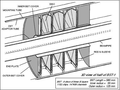
Figure 2b : H1 Backward Silicon Tracker
2.2. Readout Electronics
Altogether there are 230,000 channels which are read out by custom-built chips and circuit VMEbus boards. The complete readout chain breaks down into the following 5 basic elements:
Each chip is fabricated in a 1 um SACMOS (self-aligned CMOS) process with a 12.5 MHz switching rate and a readout speed of up to 4 MHz. This comfortably allows a 2000:1 multiplexing within the 800 us readout time. The total power consumption of a single chip, including the pipeline running at 10 MHz, is less than 40 mW, whilst functionality with 2 um CMOS prototypes has been maintained up to 100 krad (1 kGy) integrated dose from a Co60 source, the equivalent to 10 years of operation at H1; the finer SCAMOS process will further improve the radiation hardness and give larger gain and improved stability.
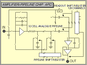
Figure 3 : Amplifier-Pipeline Readout Chip
A total of 14 signals are necessary to control the pipeline and the shift register of the sequential readout. These signals are generated by a 'Decoder' chip which needs just 4 input lines. In both the 'sample' mode, when the information per 96 ns bunch crossing is stored into the pipeline capacitors, and in the 'readout' mode, when the information of a given time slice is read out sequentially at 2.5 MHz, the two phases of the clock are directly passed to the APC.
Figure 4 shows an overview of the OnSiRoC. The data are digitised by 10 MHz, 12-bit FADCs and passed to a custom hit detector with programmable thresholds and cluster widths. For each channel and each pipeline buffer a pedestal value is stored in RAM. Both sequencer and pedestal RAMs are downline-loadable from battery backup memory either over the VMEbus or locally. Each pedestal is individual. The sequencer RAMs are configured identically for all controllers. Four data lines enable each unit to read out up to 8192 channels. Each module is of an elongated-standard single-width, double-height (6U) VMEbus size with a "piggy-back" expansion.
By virtue of the OnSiRoCs, some 2.5 Mbits of raw data information can be reduced to about 3-4 Kbytes from the CST and BST detectors. In addition, for test purposes, the pedestal memory can be used to verify all of the basic readout functionality of a particular channel via generated pattern blocks or simulated digital pulses.
2.2.3 Sequencer
The sequencer, of an OnSiRoC module is used to store the intricate command sequences for controlling the APC. Sequences are arranged so that each sequence has a unique successor, with the possibility of endless loop command sequences interrupted by a trigger, eg when sampling. Thus, once the sequencer is loaded, a single command issued over the VMEbus can instigate the functional mode of operation on the APC.
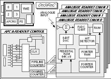
Figure 4 : OnSiRoC VMEbus Readout Controller
2.3. Data Acquisition
In order to realise fully the integration of the Silicon tracker readout electronics into the H1 data acquisition, a coherent architecture is established consistent with the rest of the system.
2.3.1 Overview of the current H1 data acquisition system
The H1 data acquisition system has been described on several occassions elsewhere [5]. A modular multi-processing environment has been designed around the IEEE VMEbus standard [1]. Several subdetector assemblies are read out in parallel by arrays of FADCs and DSPs before being merged into a central coordinating framework. Currently events of size 60 Kbytes can be coordinated with 12 branch-partitions at rates of 200 Hz via a VMEtaxi dual optical fibre ring. A parallel-filter farm of 32 RISC processors, with a performance equivalent to 20 IBM-3090 units, performs online reconstruction as well as providing a final level of full-event triggering [12]. The complete experiment is architectured so that graphics-orientated Macintosh stations provide a platform for both system operation and software development.
VMEtaxi modules can connect VMEbus crates over several kilometres with multimode 100/140 um, graded index, optic fibres [2]. 4]. There are many interesting analogies with the future international standard SCI [13]. During the early operation of H1, 25 MHz 68020 based boards were used with 125 MHz taxi chips. The upgraded "Mark-2" modules (VMExi2) are able to exploit 50 MHz 68030 processors and 250 MHz taxi chips so that, by using double fibre-optic links in parallel, transfer rates of over 50 Mbytes/s are possible [3]. The link reliability has been tested to a bit error rate of less than 1 in 1013. Program memory is provided for by 128 Kbytes of on-board dual-ported static ram, whereas EPROM and EEPROM cater for firmware storage and configuration parameters. Moreover, the on-board extension ram can capitalise on the latest 4 MBit SRAMs in order to furnish 2 Mbytes of data memory. As a result the VMExi2 can be regarded as "3 boards in one" providing processing power, optic-fibre interconnectivity (independent of distance) and high-capacity data memory on a single-width VMEbus card.
The VMExi2 was commissioned into the H1 data acquisition system during the Spring of 1993, using 175 MHz taxi chips to achieve 33 Mbytes/s peak transfer rates.
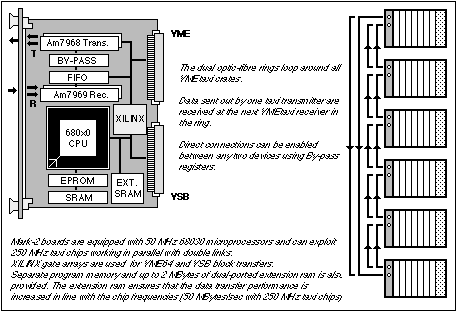
Figure 5 : VMEtaxi Mark-2
2.3.2 Silicon Tracker Data Acquisition Architecture
There are certain other constraints which also affect the design and development of the Silicon Tracker readout, namely:
An optimised scenario is shown in 14]. Naturally the system is flexible enough to embed the latest generation of 68040 CISC-based boards [15].
The DPM 8242 memory boards provide the necessary buffers for readout and monitoring purposes [16]. In addition some 10 MBytes are required for the fast access of stored pedestal and sequencer RAM values together with readout configurations.
Macintosh computers (Quadra series) are employed to remain compatible with the rest of the H1 system for software development and operator control. One device is primarily responsible for the global operation of the data acquisition, a second provides event displays and histogram monitoring and a third takes care of the monitoring of slow control information using LabVIEW [17]. Macintosh personal computer access is through MacVEE [18] or, if 32-bit access is required, through MAC 7212 [19]. The bandwidths of VMEbus in the master crate for the combined readout, processing and monitoring should not be a limitation with final event sizes of just 3 KBytes. Existing software development tools [20] and techniques [21] as used in the rest of the data acquisition system are exploited. Data quality can be monitored via event displays and histograms of, for example, pedestal and noise values, signal to noise ratios, clusters, radiation ageing (via the APC), etc., all with purpose-written programs layered on top of the existing base software packages of the H1 data acquisition system. Much of the binning and monitoring is carried out in dedicated tasks which execute permanently within the cost-effective VMEbus processors, thereby leaving the Macintosh as the graphical user interface. Such a solution has the added advantage that the VMEbus part runs as a self-contained entity, according to the protocol of the complete experiment, and is able to update the monitoring data sent to the rest of the acquisition system independent of the functionality of a local interface station.
Finally the Subsystem Trigger Control Crate handles the standard H1 triggering protocol [22].
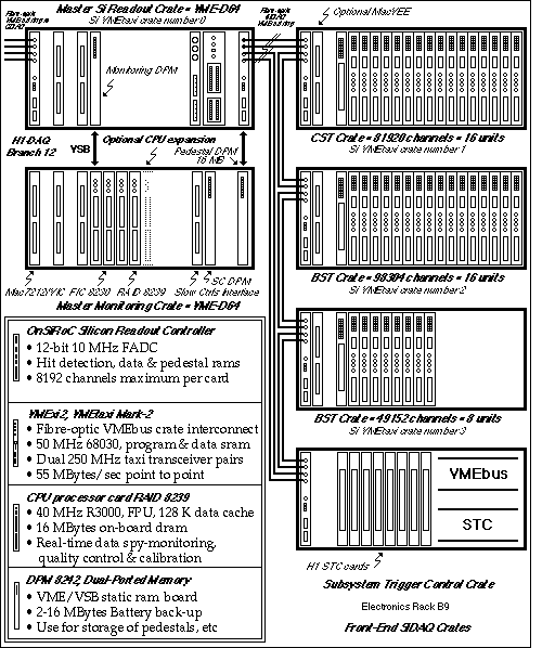
Figure 6 : Data Acquisition Readout Layout for the H1 Silicon Tracker Detectors