


Next: About this document
Up: Optical Analog Readout and
Previous: Optical Fibers and Connectors
References
- 1
- Delphi-Collaboration,
G. Anzivino et al., Nucl.Instr. Meth. A263 (1988) 215.
- 2
- Aleph-Collaboration,
G. Batignani et al., Nucl.
Instr. Meth. A315 (1992) 121 and CERN-PPE/95-017 submitted to Nucl. Instr.
Meth.
- 3
- Opal-Collaboration, P. Allport et al., Nucl. Instr. Meth.
A324 (1993) 34 and Nucl. Instr. Meth. A346 (1994) 476.
- 4
- CDF-Collaboration,
B. Barnett et al., Nucl. Instr. Meth.
A315 (1992) 121, D. Amidei et al., Nucl.
Instr. Meth. A342 (1994) 252, and Nucl. Instr. Meth. A350 (1994) 73;
S.
Tkaczyk et al., Nucl. Instr. Meth. A342 (1994) 240.
- 5
- Mark II-Collaboration, C. Adolphsen et al., Nucl.Instr. Meth.
A313 (1992) 63.
- 6
- L3-Collaboration,
M. Acciarri et al.,
CERN-PPE/94-122 , and Nucl. Instr. Meth. A360 (1995) 103.
- 7
- A prototype version with 12
channels (APC12) has been described in:
R. Horisberger and D. Pitzl, Nucl.
Instr. Meth. A326 (1993) 92.
- 8
- J. Bürger et al., Technical proposal to
build silicon tracking detectors for H1, H1 internal report 226 (1992) and DESY
PRC92/01;
D. Pitzl et al., IEEE Nucl. Science Symp. 1992, unpublished.
- 9
- O. Adriani et al., Nucl. Instr. Meth. A342 (1994) 181.
- 10
- E. Gatti, P.F. Manfredi and V. Speziali, Nucl. Instr. Meth.
226 (1984) 1163,
M. Leone et al., Nucl. Instr. Meth. A333 (1993) 519.
- 11
- D. Pitzl et al., Nucl. Instr. Meth. A348 (1994) 454
C.S.E.M. SA, CH 2007 Neuchâtel, Maladière 71, Case Postale 41,
Switzerland.
- 12
- J. Bürger et al., Proc. Wire Chamber Conference Vienna,
1995 and DESY 95-049.
- 13
- Faselec AG, Philips Semiconductor, Binzstr. 44,
CH 8045 Zürich, Switzerland.
- 14
- W. Erdmann and S. Streuli; Swiss Patent Nr 3026/94-2.
- 15
- Huber & Suhner, Degersheimerstr. 14, CH 9100 Herisau, Switzerland.
- 16
- Ciba Geigy, CH 4000 Basel, Switzerland.
- 17
- Polyscience AG, Riedstr. 13, CH 6330 Cham, Switzerland.
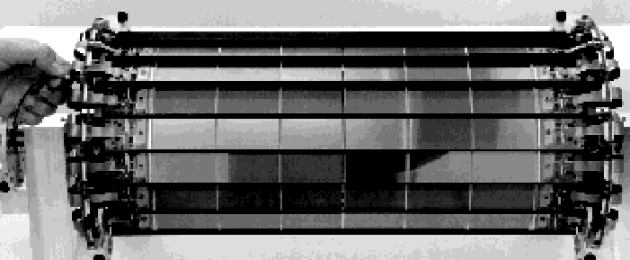
Figure: Half shell of the
Central Silicon Tracker of H1.
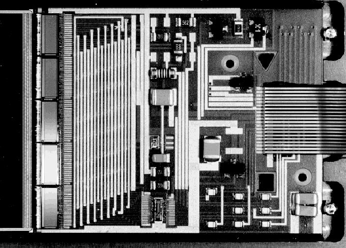
Figure: p-side of the hybrid made from
635  m
m  . Left: Five preamplifier chips (APC128). Low center: Decoder Chip.
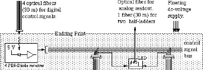
Figure: Schematic layout of
the electrical and optical readout and control.
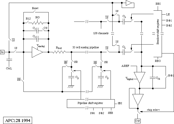
Figure: Simplified diagram of APC128 chip.
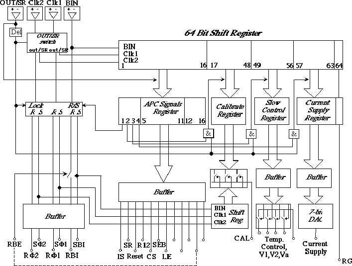
Figure: Layout of Decoder Chip.
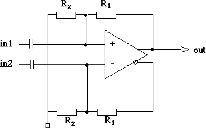
Figure: Circuit diagram of the input stages
of the decoder chip. The capacitors are external to the decoder chip.
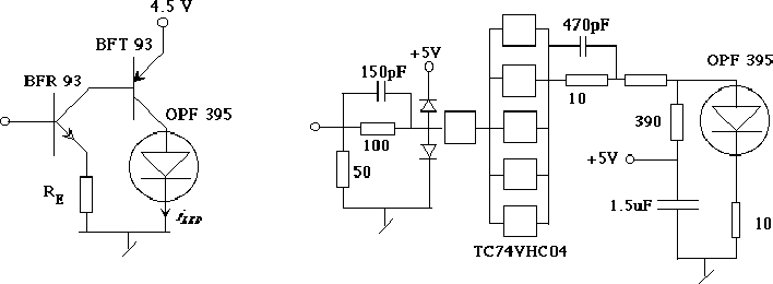
Figure: Circuit diagram of the electrical-optical
converters. Left: Analog signal driver situated on the hybrid (with the exception of the
LED). Power consumption 50 mW. Right: Digital signal driver
situated 34 m apart from the detector.
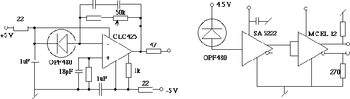
Figure: Circuit diagram of the optical-electrical
converters. Left: Analog signal receiver situated 34 m
apart from the detector. Right: Digital signal receiver situated
on a printed circuit at the end of the detector. Power consumption 250
mW.
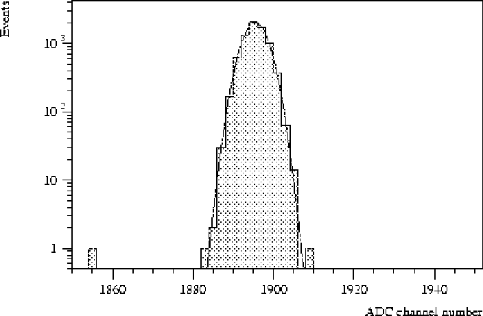
Figure: Distribution of measurements of a
reference voltage (2V) transmitted
through the optical readout chain and digitised
with a 12 bit FADC. The distribution is purely Gaussian with an r.m.s of 2.9
bits. For comparison: Signals from the APC128 have a noise contribution of 32
bits.
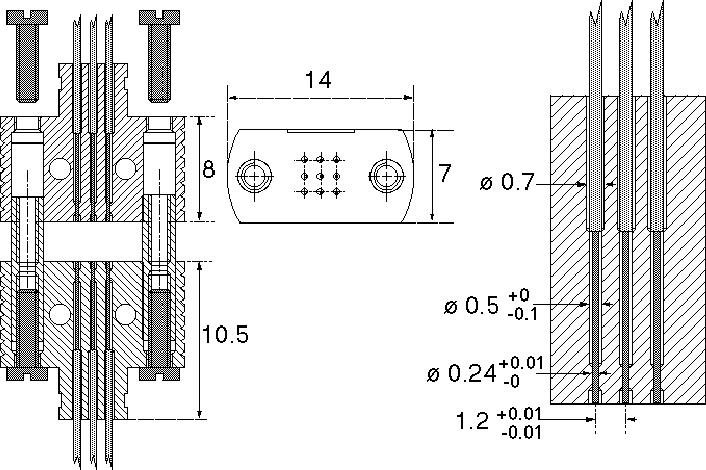
Figure: Pair of optical multiconnectors (left) and
enlarged view of the central part with fibers glued in (right).
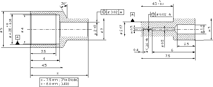
Figure: Left: Housing for diode. Right: fiber end.
Markus Kausch
Tue Jun 25 14:34:46 MST 1996